Category
page 1Semiconductor structures
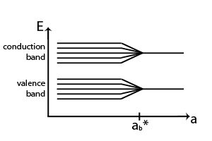
quantum dot
nano-scale semiconductor particle subject to quantum effects
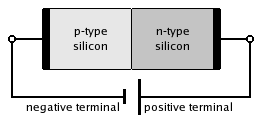
p–n junction
semiconductor–semiconductor junction, formed at the boundary between a p-type and n-type semiconductor
depletion region
insulating region in a conductive, dopend semiconductor
silicon on insulator
semiconductor manufacturing process

heterojunction
A heterojunction is an interface between two layers or regions of dissimilar semiconductors. These semiconducting materials have unequal band gaps as opposed to a homojunction. It is often advantageous to engineer the electronic energy bands in many solid-state device applications, including semiconductor lasers, solar cells and transistors. The combination of multiple heterojunctions together in a device is called a heterostructure, although the two terms are commonly used interchangeably. The requirement that each material be a semiconductor with unequal band gaps is somewhat loose, especial
quantum well
concept in quantum mechanics
Schottky barrier
potential energy barrier in metal-semiconductor junctions
quantum wire
an electrically conducting wire in which quantum effects influence the transport properties
Ohmic contact
non-rectifying electrical junction: a junction between two conductors that has a linear current–voltage (I-V) curve as with Ohm's law
metal–semiconductor junction
type of electrical junction
surface states
electronic states at the surface of materials
band diagram
diagram plotting various key electron energy levels as a function of some spatial dimension, which is often denoted x
homojunction
thumb|400px|right|A homojunction PN junction. The band at the interface is continuous. In forward bias mode, the [[depletion width decreases. Both p and n junctions are doped at a 1e15/cm3 doping level, leading to built-in potential of ~0.59 V. Observe the different Quasi Fermi levels for conduction band and valence band in n and p regions (red curves).]]
Shallow trench isolation
integrated circuit
Metal gate
Semiconductor structure
quantum heterostructure
Gate dielectric
field-effect transistor

gate oxide
dielectric layer of a MOSFET separating the source and drain from the gate terminal
field effect
Applied electric field conductivity change
p–n junction isolation
method used to isolate components by surrounding them with reverse biased p–n junctions